Author Affiliations
Abstract
1 Key Laboratory for Information Science of Electromagnetic Waves (MoE), Department of Communication Science and Engineering, Fudan University, Shanghai 200433, China
2 National Institute of LED on Silicon Substrate, Nanchang University, Nanchang 330096, China
In recent studies, visible light communication (VLC) has been predicted to be a prospective technique in the future 6G communication systems. To suit the trend of exponentially growing connectivity, researchers have intensively studied techniques that enable multiple access (MA) in VLC systems, such as the MIMO system based on LED devices to support potential applications in the Internet of Things (IoT) or edge computing in the next-generation access network. However, their transmission rate is limited due to the intrinsic bandwidth of LED. Unfortunately, the majority of visible light laser communication (VLLC) research with beyond 10 Gb/s data rates concentrates on point-to-point links, or using discrete photodetector (PD) devices instead of an integrated array PD. In this paper, we demonstrated an integrated PD array device fabricated with a Si-substrated GaN/InGaN multiple-quantum-well (MQW) structure, which has a array of micro-PD units with a common cathode and anode. This single-integrated array successfully provides access for two different transmitters simultaneously in the experiment, implementing a MIMO-VLLC link at 405 nm. The highest data rate achieved is 13.2 Gb/s, and the corresponding net data rate (NDR) achieved is 12.27 Gb/s after deducing the FEC overhead, using 2.2 GHz bandwidth and superposed PAM signals. Furthermore, we assess the Huffman-coded coding scheme, which brings a fine-grain adjustment in access capacity and enhances the overall data throughput when the user signal power varies drastically due to distance, weather, or other challenges in the channel condition. As far as we know, this is the first demonstration of multiple visible light laser source access based on a single integrated GaN/InGaN receiver module.
Photonics Research
2024, 12(4): 793

Author Affiliations
Abstract
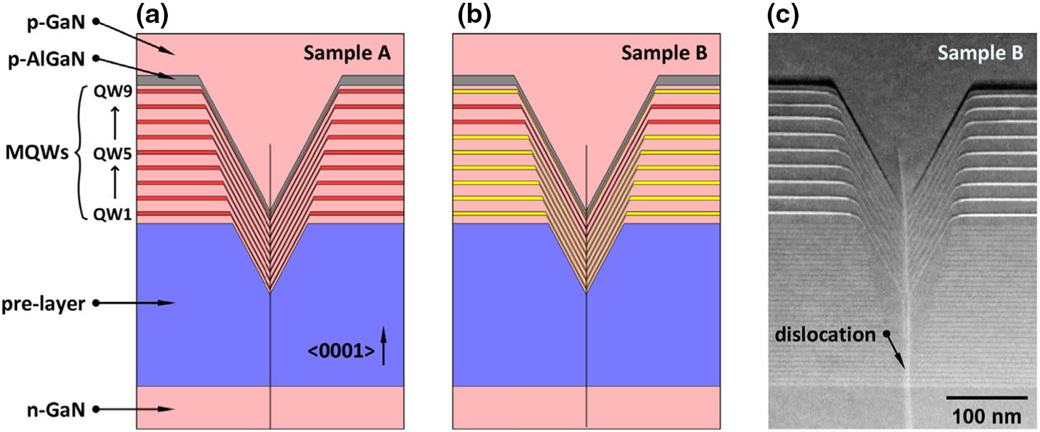
Although the 5G wireless network has made significant advances, it is not enough to accommodate the rapidly rising requirement for broader bandwidth in post-5G and 6G eras. As a result, emerging technologies in higher frequencies including visible light communication (VLC), are becoming a hot topic. In particular, LED-based VLC is foreseen as a key enabler for achieving data rates at the Tb/s level in indoor scenarios using multi-color LED arrays with wavelength division multiplexing (WDM) technology. This paper proposes an optimized multi-color LED array chip for high-speed VLC systems. Its long-wavelength GaN-based LED units are remarkably enhanced by V-pit structure in their efficiency, especially in the “yellow gap” region, and it achieves significant improvement in data rate compared with earlier research. This work investigates the V-pit structure and tries to provide insight by introducing a new equivalent circuit model, which provides an explanation of the simulation and experiment results. In the final test using a laboratory communication system, the data rates of eight channels from short to long wavelength are 3.91 Gb/s, 3.77 Gb/s, 3.67 Gb/s, 4.40 Gb/s, 3.78 Gb/s, 3.18 Gb/s, 4.31 Gb/s, and 4.35 Gb/s (31.38 Gb/s in total), with advanced digital signal processing (DSP) techniques including digital equalization technique and bit-power loading discrete multitone (DMT) modulation format.
GaN-based LED LED array VLC V-pit sidewall quantum well high-frequency response Opto-Electronic Science
2023, 2(5): 230005

Author Affiliations
Abstract
1 Key Laboratory for Information Science of Electromagnetic Waves (MoE), Fudan University, Shanghai 200433, China
2 Shanghai Engineering Research Center of Low-Earth-Orbit Satellite Communication and Applications, Shanghai 200433, China
3 Shanghai Collaborative Innovation Center of Low-Earth-Orbit Satellite Communication Technology, Shanghai 200433, China
4 National Institute of LED on Silicon Substrate, Nanchang University, Nanchang 330096, China
5 Peng Cheng Laboratory, Shenzhen 518055, China
6 e-mail:
7 e-mail:
8 e-mail:
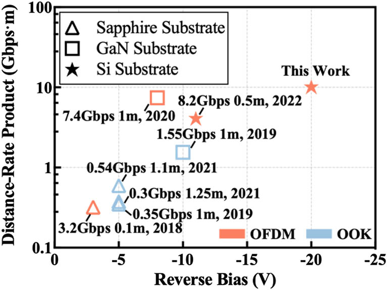
Visible light communication (VLC) has emerged as a promising communication method in 6G. However, the development of receiving devices is much slower than that of transmitting devices, limited by materials, structures, and fabrication. In this paper, we propose and fabricate an InGaN/GaN multiple-quantum-well-based vertical-structure micro-LED-based photodetector (μPD) on a Si substrate. A comprehensive comparison of the photoelectrical performance and communication performance of three sizes of μPDs, 10, 50, and 100 μm, is presented. The peak responsivity of all three μPDs is achieved at 400 nm, while the passband full-widths at half maxima are 87, 72, and 78 nm for 10, 50, and 100 μm μPDs, respectively. The cutoff bandwidth is up to 822 MHz for 50 μm μPD. A data rate of 10.14 Gbps is experimentally demonstrated by bit and power loading discrete multitone modulation and the proposed digital pre-equalizer algorithm over 1 m free space utilizing the self-designed 50 μm μPD array as a receiver and a 450 nm laser diode as a transmitter. This is the first time a more than 10 Gbps VLC system has been achieved utilizing a GaN-based micro-PD, to the best of our knowledge. The investigation fully demonstrates the superiority of Si substrates and vertical structures in InGaN/GaN μPDs and shows its great potential for high-speed VLC links beyond 10 Gbps.
Photonics Research
2022, 10(10): 2394

Author Affiliations
Abstract
National Institute of LED on Silicon Substrate, Nanchang University, Nanchang 330096, China
Indium gallium nitride (InGaN)-based light-emitting diodes (LEDs) are considered a promising candidate for red-green-blue (RGB) micro displays. Currently, the blue and green LEDs are efficient, while the red ones are inefficient for such applications. This paper reports our work of creating efficient InGaN-based orange and red LEDs on silicon(111) substrates at low current density. Based on the structure of InGaN yellow LEDs, by simply reducing the growth temperature of all the yellow quantum wells (QWs), we obtained 599 nm orange LEDs with peak wall-plug efficiency (WPE) of 18.1% at . An optimized QW structure was proposed that changed two of the nine yellow QWs to orange ones. Compared with the sample containing nine orange QWs, the sample with two orange QWs and seven yellow QWs showed similar emission spectra but a much higher peak WPE up to 24.0% at with a wavelength of 608 nm. The improvement of peak WPE can be attributed to the improved QW quality and the reduced active recombination volume. Subsequently, a series of efficient InGaN-based orange and red LEDs was demonstrated. With further development, the InGaN-based red LEDs are believed to be attainable and can be used in micro LED displays.
Photonics Research
2020, 8(11): 11001671
Author Affiliations
Abstract
1 National Institute of LED on Silicon Substrate, Nanchang University, Nanchang 330096, China
2 Nanchang Yellow Green Lighting Company Limited, Nanchang 330096, China
3 e-mail: liujunlin@ncu.edu.cn
Realization of efficient yellow-light-emitting diodes (LEDs) has always been a challenge in solid-state lighting. Great effort has been made, but only slight advancements have occurred in the past few decades. After comprehensive work on InGaN-based yellow LEDs on Si substrate, we successfully made a breakthrough and pushed the wall-plug efficiency of 565-nm-yellow LEDs to 24.3% at 20 A/cm2 and 33.7% at 3 A/cm2. The success of yellow LEDs can be credited to the improved material quality and reduced compressive strain of InGaN quantum wells by a prestrained layer and substrate, as well as enhanced hole injection by a 3D pn junction with V-pits.
Photonics Research
2019, 7(2): 02000144
南昌大学国家硅基LED工程技术研究中心, 江西 南昌 330047
利用金属有机化合物气相外延沉积技术在2 inch (5.08 cm) Si(111)图形衬底上生长了GaN外延薄膜,在Al组分渐变AlGaN缓冲层与GaN成核层之间引入了AlN插入层,研究了AlN插入层对GaN薄膜生长的影响。结果表明,随着AlN插入层厚度的增加,GaN外延膜(002)面与(102)面X射线衍射摇摆曲线半峰全宽明显变小,晶体质量变好,同时外延膜在放置过程中所产生的裂纹密度逐渐减小直至不产生裂纹。原因在于AlN插入层的厚度对GaN成核层的生长模式有明显影响,较厚的AlN插入层使GaN成核层倾向于岛状生长,造成后续生长的n-GaN外延膜具有更多的侧向外延成分,从而降低了GaN外延膜中的位错密度,减少了GaN外延膜中的残余张应力。同时还提出了一种利用荧光显微镜观察黄带发光形貌来表征GaN成核层形貌和生长模式的新方法。
薄膜 氮化镓 氮化铝插入层 硅衬底 黄带
光电技术与系统教育部重点实验室, 重庆大学 光电工程学院, 重庆 400030
提高LED芯片的出光效率是解决LED光源大功率化和可靠性的根本。根据LED芯片所用衬底材料的不同, 总结了近年来提高GaN基LED出光效率的研究进展, 介绍了新的设计思路、工艺结构与制备方法。并从材料结构和衬底选取方面, 对LED芯片未来的发展趋势进行了展望。
发光学 出光效率 衬底图案化 衬底转移 垂直结构 luminescence LED LEDs light extraction efficiency patterned substrate substrate removal vertical structure


